High-Voltage Serial Programmer – Rescue AVR Chips
Imagine you accidentally disable the reset line, or disable the internal clock of your AVR chip – you’ve bricked your microcontroller. The HVSP1 can reset the device back to factory settings, automatically.
Motivation
Some of my ATtiny85 BlinkSticks no longer accept serial programming because of issues with undervoltage from a slow-decay power supply. Those issues have been resolved, and brown-out detect (BOD) fuses are now enabled. However, a handful went haywire and need the NAND fuses reset so they accept SPI and JTAG programming again. Let’s fix that.
High-Voltage Serial Programmer
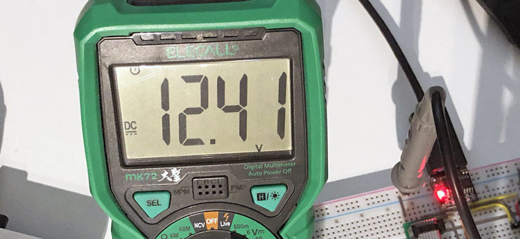
The voltage we’re talking about is only 12V. AVR chips have a backdoor to recover them, and precise timing and 12V are all that is needed to backdoor into bricked chips.
There are many neat articles on building HV programmers for and with Atmel AVR microcontrollers. One uses a 12V A23 battery (with only 55 mAh) and a common transistor to achieve the 12V. Another design uses a barrel jack and an external 12V power supply with a voltage regulator to supply both 5V and 12V. Others even use a diode-capacitor charge pump using two clock sources from an Arduino. Let’s expand on the charge-pump idea with a dedicated IC chip.
How Charge Pumps Work
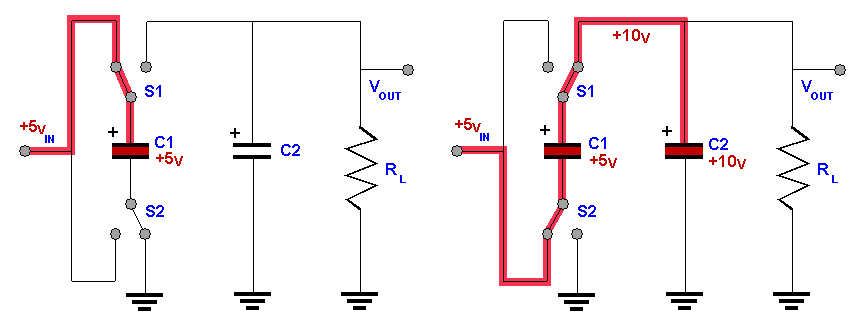
Charge pumps – also called switching voltage regulators – are fascinating. Without inductors or transformers, and just by switching solid-state components at the right frequency in relation to capacitance, it is possible to double, triple, or n-multiply the source voltage. Of course, the current is very low, but we only need a handful of milliamps for a brief duration to reset the fuses. The simplest DC-DC charge pump is the Dickson Charge Pump.
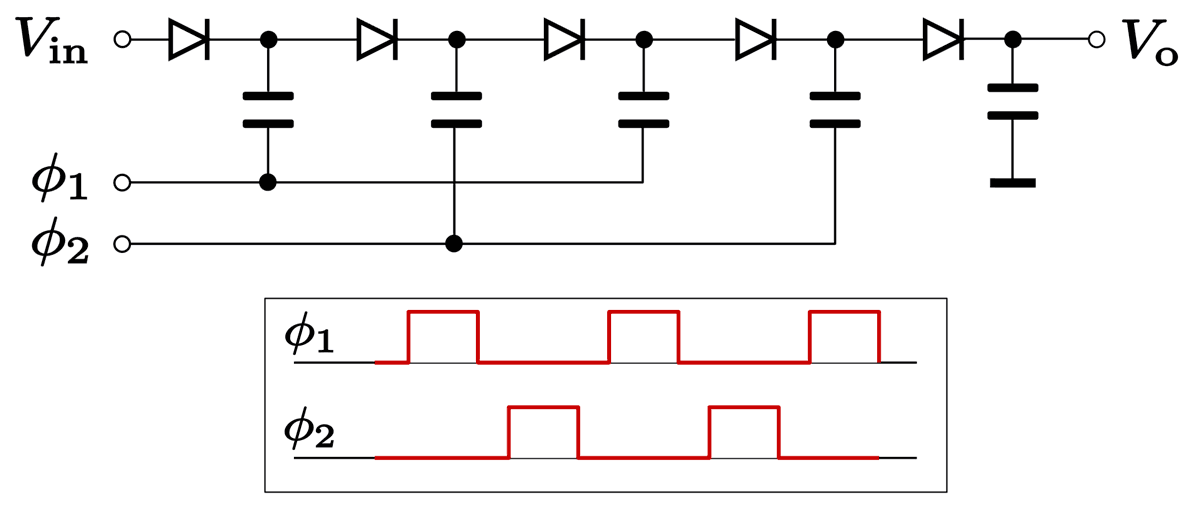
A multi-stage Dickson charge pump with just diodes and capacitors needs two clock signals 180 degrees out of phase to make the charge cascade propagate. An alternative is to use one clock source with some NOT logic to invert the original signal into two signals. The design below is a 4x voltage multiplier.
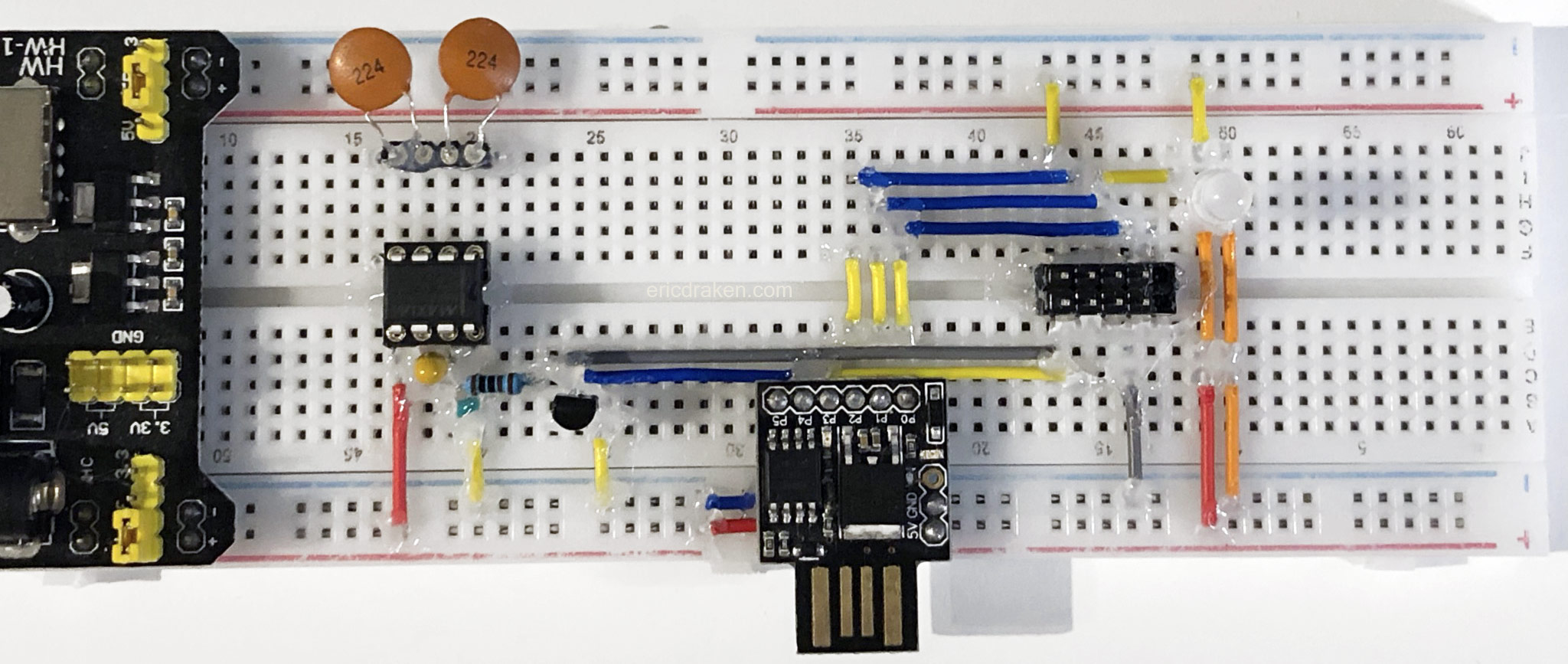
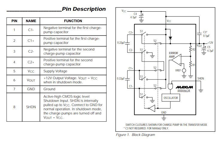
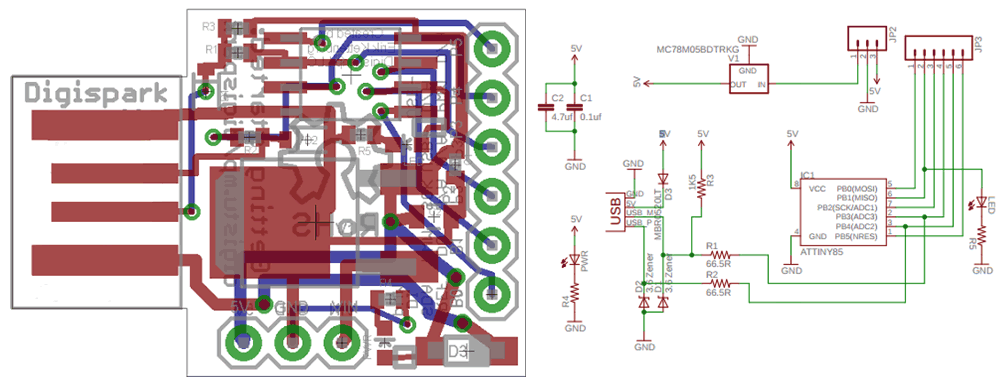
The MAX662A and LTC1263 are excellent charge pump ICs. I’ll be using the Maxim MAX662A with two external capacitors in my design. Here is the schematic:
To switch between 0V and 12V, we’ll use a simple transistor to enter and exit HVSP mode.
Digispark ATtiny85 as an HV Serial Programmer
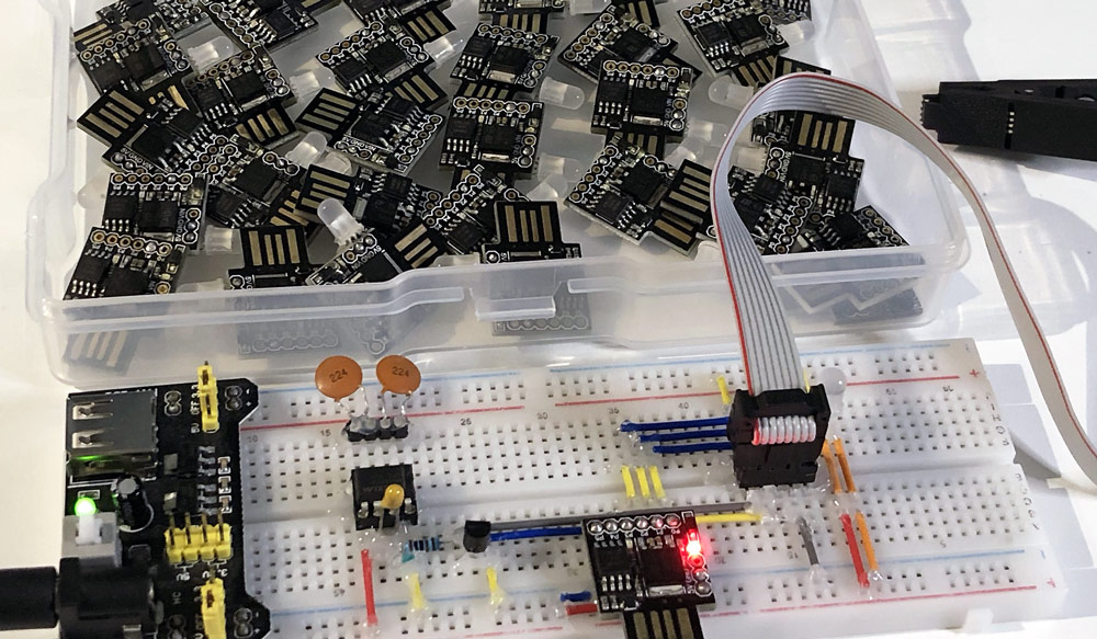
Having dozens of 8-bit ATtiny85 Digisparks at hand, I’ll use one as an HV programmer to program other ATtiny85s. It’s perfect for the job: it’s powered by the USB bus, has most of the passive components already, and lends itself to customization. First, let’s explore the schematic of the Digispark by Digistump.
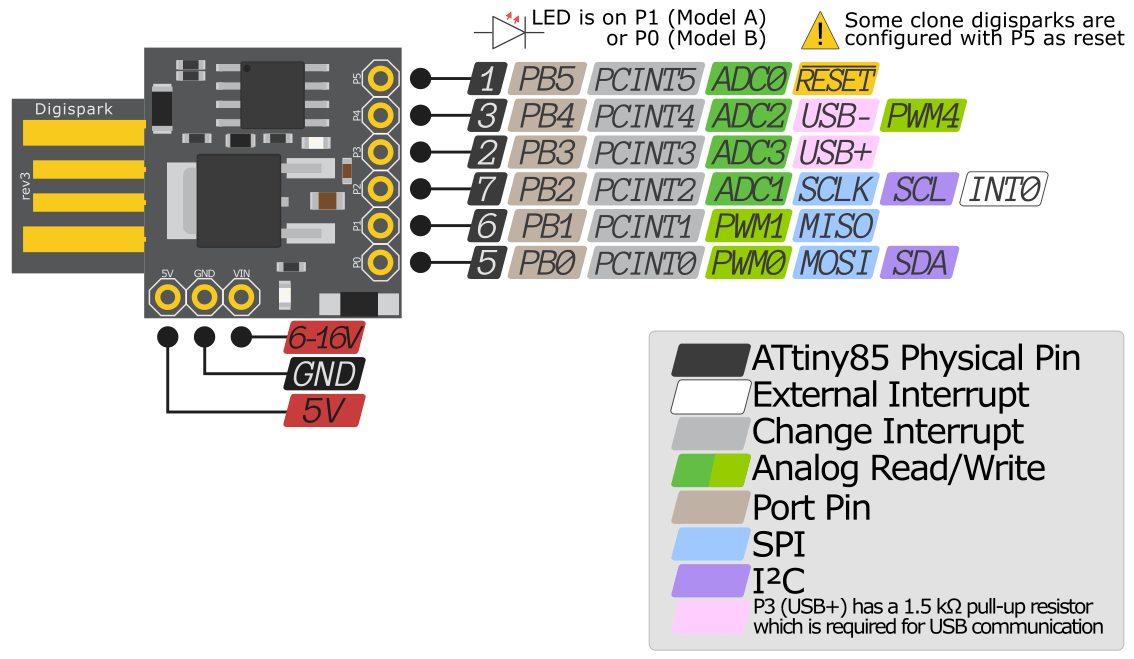
Here is an ATtiny85 Digistump pinout reference.
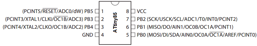
Here is a pin reference for the 8-pin ATtiny85 DIP.
It should be fairly easy to incorporate the MAX662A, a couple of 0.22uF 5%-tolerance capacitors (224J), and a transistor into the above schematic. It looks like VIN and PB5 (reset) will be left floating. More on that later.
Atmel AVR High-Voltage Protocol
Simply put, you can apply 0V and then 12V to the target reset pin (PB5) at any time to enter HVSP mode.
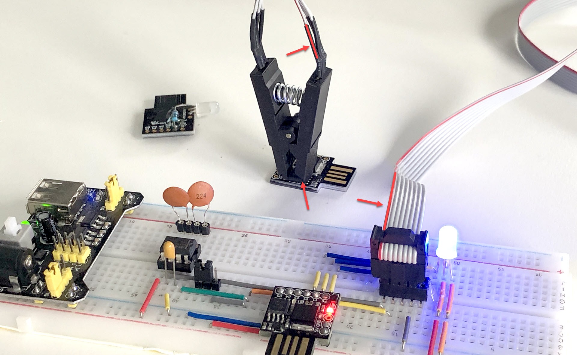
Using this simple trick, and by keeping the power on continuously, I can flash many ATtiny85 chips just by attaching and removing a SOIC8 test clip. No need to toggle power. This is the advantage of this design over others. Also, I use colored LEDs for some flare.
Drawing inspiration from this article, we can learn a lot about the protocol. See below.
The protocol follows a similar pattern to the following:
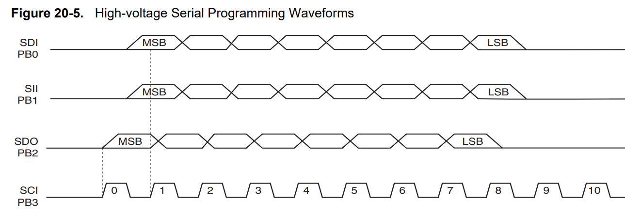
One exciting discovery from this blog is that in addition to resetting the fuses, a chip may need to be erased if it is super bricked with the Lock Bit Protection on. Let’s get to some code.
Hardware and Schematics
Not much is needed to make an HV serial programmer: just a few capacitors, a neat charge-pump IC, a run-of-the-mill transistor, a resistor, a Digistump, and the SOIC8 connector. Added for fun is an APA106 NeoPixel LED to show the flashing status more pleasingly.
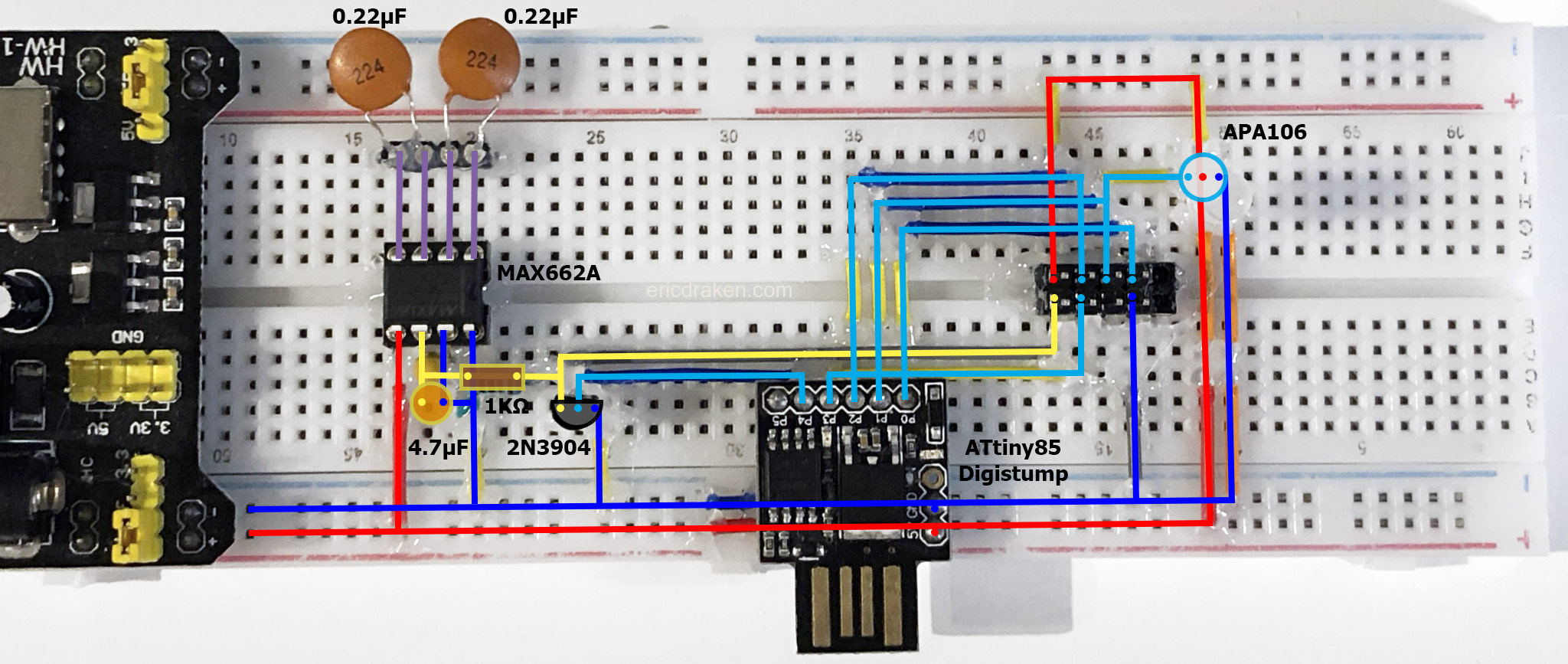
Parts
- 1x ATtiny85 Digispark
- 1x MAX662A charge-pump IC
- 1x 2N3904 NPN transistor
- 1x 1KΩ resistor
- 2x 0.22μF 5% capacitors – 224J marking
- 1x 4.7μF polarized capacitor2 – 475 marking
- 1x DIP 2×4 pin connector
- 1x SOIC8 clip, ribbon cable, and 2×4 ribbon female connector
- 1x APA106 NeoPixel LED (optional)
Capacitor Information
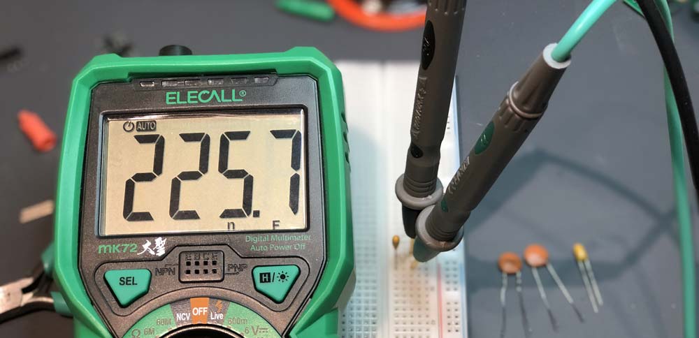
But, what kind of capacitors should be used? I use ceramic 224J (0.22uF at 5% tolerance). Here is a quick reference3 of the types of capacitors:
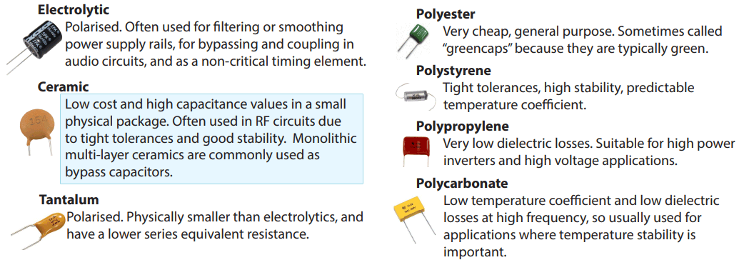
Not being one to chance the values and ratings of the passive components, I took this time to verify the values of the capacitors. Here I see that at room temperature this capacitor, which is rated at 0.22μF, is reading 226nF, so it is viable.
Software
Let’s get into the driver logic that resets the fuses, erases the flash, and rescues your bricked AVR chips.
Enter HVSP Mode
How do we enter HVSP mode? With a little bit of timing, the procedure is as follows (Source: Atmel):
- Set Prog_enable pins listed in Table 20-14 to “000”, RESET pin and VCC to 0V.
- Apply ~5V between VCC and GND. Ensure that VCC reaches at least 1.8V within the next 20 μs.
— No minimum time required between step 2 and 3 — - Wait 20 – 60 μs, and apply 11.5 – 12.5V to RESET.
- Keep the Prog_enable pins unchanged for at least 10 μs after the High-voltage has been applied to ensure the Prog_enable Signature has been latched.
- Release the Prog_enable[2] pin to avoid drive contention on the Prog_enable[2]/SDO pin.
- Wait at least 300 μs before giving any serial instructions on SDI/SII.
- Exit Programming mode by power the device down or by bringing RESET pin to 0V.
Again, in code,
1 2 3 4 5 6 7 8 9 10 11 12 13 14 15 | void enterHVSPMode() { pinMode(SDO, OUTPUT); // Set SDO to output digitalWrite(RST, HIGH); // 12V off digitalWrite(SDI, LOW); digitalWrite(SII, LOW); digitalWrite(SDO, LOW); delayMicroseconds(30); // Wait long enough for target chip to see rising edge digitalWrite(RST, LOW); // Set MAX662A SHDN to low for normal operation = 12V on delayMicroseconds(10); pinMode(SDO, INPUT); // Set SDO to input delayMicroseconds(300); // Next, read signature } |
Chip Erase
From the Atmel AVR spec sheet for the ATtiny series,
The Chip Erase will erase the Flash and EEPROM memories plus Lock bits. The Lock bits are not reset until theProgram memory has been completely erased. The Fuse bits are not changed. A Chip Erase must be performedbefore the Flash and/or EEPROM are re-programmed. – Microchip
Here is the Chip Erase procedure.
1 2 3 4 5 6 | // See table 20-16 from the datasheet on ATtiny85 void chipErase() { shiftOut(0b10000000, 0b01001100); shiftOut(0b00000000, 0b01100100); shiftOut(0b00000000, 0b01101100); } |
Main Loop
When powered on, the AVR timings and delays are initialized, then the pins are set to output mode. When completed, a yellow color illuminates.
The main loop starts by initiating the HVSP mode. If the ATtiny85 is connected via the SOIC8 clip, then the chip is erased and the fuses are reset. If successful, then a green light will blink rapidly. If unsuccessful, then a red light will blink rapidly. The blinking will continue until the SOIC8 clip is disconnected, and happily there will not be an infinite loop of chip flashing. The ATtiny85 SOIC8 clip must be disconnected and reconnected for the flashing to reinitiate. This way many chips can be flashed without power-cycling the circuit.
1 2 3 4 5 6 7 8 9 10 11 12 13 14 15 16 17 18 19 20 21 22 23 24 25 26 27 28 | int main(void) { init(); // Arduino init biolerplate setup(); yellow(); for(;;) { enterHVSPMode(); if(isSOICConnected()) { red(); delay(1000); chipErase(); yellow(); delay(1000); flashFuses(); } else { error = 2; // The SOIC8 clip is not connected } do { updateStatus(); } while(fusesSetCorrectly()); leaveHVSPMode(); } return 0; } |
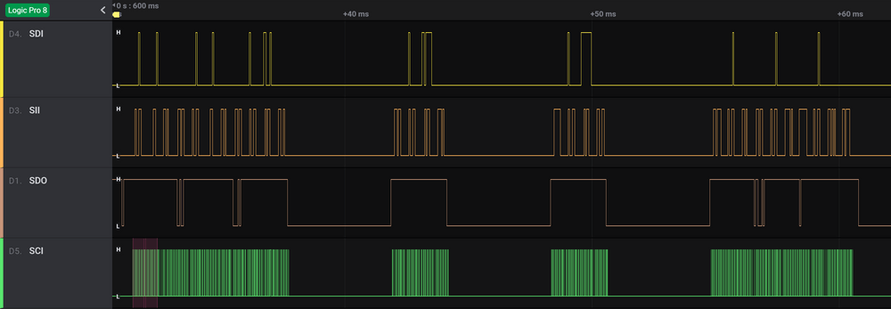
Demo
Full Code
Below is the complete C++ code. It’s verbose on purpose so it is easy to follow and maintain.
0x62 (Int. RC Osc. 8 MHz; Start-up time PWRDWN/RESET: 6 CK/14 CK + 64 ms; [CKSEL=0010 SUT=10]).I’ve found this value keeps the chips bricked. Interrogating several factory ATtiny85 Digisparks, they all seem to have 0xF1 as the low fuse which works brilliantly (PLL Clock; Start-up time PWRDWN/RESET: 16K CK/14 CK + 64 ms; [CKSEL=0001 SUT=11]).
Let’s use the low fuse of 0xF1 going forward.
1 2 3 4 5 6 7 8 9 10 11 12 13 14 15 16 17 18 19 20 21 22 23 24 25 26 27 28 29 30 31 32 33 34 35 36 37 38 39 40 41 42 43 44 45 46 47 48 49 50 51 52 53 54 55 56 57 58 59 60 61 62 63 64 65 66 67 68 69 70 71 72 73 74 75 76 77 78 79 80 81 82 83 84 85 86 87 88 89 90 91 92 93 94 95 96 97 98 99 100 101 102 103 104 105 106 107 108 109 110 111 112 113 114 115 116 117 118 119 120 121 122 123 124 125 126 127 128 129 130 131 132 133 134 135 136 137 138 139 140 141 142 143 144 145 146 147 148 149 150 151 152 153 154 155 156 157 158 159 160 161 162 163 164 165 166 167 168 169 170 171 172 173 174 175 176 177 178 179 180 181 182 183 184 185 186 187 188 189 190 191 192 193 194 195 196 197 198 199 200 201 202 203 204 205 206 207 208 209 210 211 212 213 214 215 216 217 218 219 220 221 222 223 224 225 226 227 228 229 230 231 232 233 234 235 236 237 238 239 240 241 242 243 244 245 246 247 248 249 250 251 252 253 254 255 256 | // hvsp.cpp // ATtiny85 High-Voltage Serial Fuse Resetter // Inspiration: https://sites.google.com/site/wayneholder/attiny-fuse-reset // Fuse Calc: http://www.engbedded.com/fusecalc/ // // Author: Eric Draken (https://ericdraken.com/hv-serial-programmer) // REF: https://github.com/ericdraken/digispark-firmware-attiny85 #include <Arduino.h> extern "C" { #include "apa106.h" // Source: https://github.com/ericdraken/digispark-firmware-attiny85/ // Renamed from light_ws2812.h } // These are specific to the ATtiny85 #define RST 4 // (PB4/PWM4 ) Output to the SHDN pin on the MAX662A #define SCI 3 // (PB3/CLKI ) Target Clock Input #define SDO 2 // (PB2/SCK ) Target Data Output #define SII 1 // (PB1/MISO ) Target Instruction Input #define SDI 0 // (PB0/MOSI ) Target Data Input #define LFUSE 0x646C #define HFUSE 0x747C #define EFUSE 0x666E #define LFTARGET 0xF1 // Default is 0x62, but 0xF1 works better #define HFTARGET 0xDF // BOD off by default #define EFTARGET 0xFF // ATTiny 8-pin series signatures #define ATTINY25 0x9108 // L: 0x62, H: 0xDF, E: 0xFF 8 pin #define ATTINY45 0x9206 // L: 0x62, H: 0xDF, E: 0xFF 8 pin #define ATTINY85 0x930B // L: 0x62, H: 0xDF, E: 0xFF 8 pin int error = 0; byte FuseL = 0; byte FuseH = 0; byte FuseX = 0; static volatile uint8_t led[3] = {}; byte shiftOut (byte val1, byte val2) { while (!digitalRead(SDO)); // Wait until SDO goes high int inBits = 0; unsigned int dout = (unsigned int) val1 << 2; unsigned int iout = (unsigned int) val2 << 2; for (int ii = 10; ii >= 0; ii--) { digitalWrite(SDI, !!(dout & (1 << ii))); digitalWrite(SII, !!(iout & (1 << ii))); inBits <<= 1; inBits |= digitalRead(SDO); digitalWrite(SCI, HIGH); digitalWrite(SCI, LOW); } return inBits >> 2; } void writeFuse (unsigned int fuse, byte val) { shiftOut(0x40, 0x4C); shiftOut( val, 0x2C); shiftOut(0x00, (byte) (fuse >> 8)); shiftOut(0x00, (byte) fuse); } void readFuses () { shiftOut(0x04, 0x4C); // LFuse shiftOut(0x00, 0x68); FuseL = shiftOut(0x00, 0x6C); shiftOut(0x04, 0x4C); // HFuse shiftOut(0x00, 0x7A); FuseH = shiftOut(0x00, 0x7E); shiftOut(0x04, 0x4C); // EFuse shiftOut(0x00, 0x6A); FuseX = shiftOut(0x00, 0x6E); } unsigned int readSignature () { unsigned int sig = 0; byte val; for (int ii = 1; ii < 3; ii++) { shiftOut(0x08, 0x4C); shiftOut( ii, 0x0C); shiftOut(0x00, 0x68); val = shiftOut(0x00, 0x6C); sig = (sig << 8) + val; } return sig; } void chipErase() { // See table 20-16 from the datasheet on ATtiny85 shiftOut(0b10000000, 0b01001100); shiftOut(0b00000000, 0b01100100); shiftOut(0b00000000, 0b01101100); } bool isSOICConnected() { unsigned int sig = readSignature(); return (sig == ATTINY25 || sig == ATTINY45 || sig == ATTINY85); } bool fusesSetCorrectly() { readFuses(); // Check that fuses were set properly return FuseL == LFTARGET && FuseH == HFTARGET && FuseX == EFTARGET; } void flashFuses() { writeFuse(LFUSE, LFTARGET); writeFuse(HFUSE, HFTARGET); writeFuse(EFUSE, EFTARGET); if (fusesSetCorrectly()) { error = 0; // Success } else { error = 1; // The fuses weren't set correctly } } void setup() { pinMode(SDO, OUTPUT); // Configured as input when in programming mode digitalWrite(RST, HIGH); // Set MAX662A SHDN to high (default) for "shutdown" mode = 12V off pinMode(RST, OUTPUT); pinMode(SDI, OUTPUT); pinMode(SII, OUTPUT); pinMode(SCI, OUTPUT); } void off() { led[0] = 0; led[1] = 0; led[2] = 0; apa106_sendarray_mask(&led[0], 3, _BV(apa106_pin)); } void red() { led[0] = 32; led[1] = 0; led[2] = 0; apa106_sendarray_mask(&led[0], 3, _BV(apa106_pin)); } void green() { led[0] = 0; led[1] = 32; led[2] = 0; apa106_sendarray_mask(&led[0], 3, _BV(apa106_pin)); } void yellow() { led[0] = 32; led[1] = 32; led[2] = 0; apa106_sendarray_mask(&led[0], 3, _BV(apa106_pin)); } void pulseGreen(int count) { for (int i = 0; i < count; i++) { green(); delay(50); off(); delay(50); } } void pulseYellowSlow(int count) { for (int i = 0; i < count; i++) { yellow(); delay(1000); off(); delay(1000); } } void pulseRed(int count) { for (int i = 0; i < count; i++) { green(); delay(50); off(); delay(50); } } void updateStatus() { switch(error) { case 0: { pulseGreen(5); // Success break; } case 1: { pulseRed(5); // Fuses weren't flashed properly break; } case 2: { pulseYellowSlow(1); // Waiting to connect SOIC8 clip break; } } } void enterHVSPMode() { pinMode(SDO, OUTPUT); // Set SDO to output digitalWrite(RST, HIGH); // 12V off digitalWrite(SDI, LOW); digitalWrite(SII, LOW); digitalWrite(SDO, LOW); delayMicroseconds(30); // Wait long enough for target chip to see rising edge digitalWrite(RST, LOW); // Set MAX662A SHDN to low for normal operation = 12V on delayMicroseconds(10); pinMode(SDO, INPUT); // Set SDO to input delayMicroseconds(300); // Next, read signature } void leaveHVSPMode() { digitalWrite(SCI, LOW); digitalWrite(RST, HIGH); // Set MAX662A SHDN to high (default) for "shutdown" mode = 12V off } int main(void) { init(); // Arduino init biolerplate setup(); yellow(); for(;;) { enterHVSPMode(); if(isSOICConnected()) { red(); delay(1000); chipErase(); yellow(); delay(1000); flashFuses(); } else { error = 2; // The SOIC8 clip is not connected } do { updateStatus(); } while(fusesSetCorrectly()); leaveHVSPMode(); } return 0; } |
Makefile
Run make hex to compile the hex file which can then be flashed to the ATtiny85 via a serial programmer, or uploaded via micronucleus or AVRDUDE.
1 2 3 4 5 6 7 8 9 10 11 12 13 14 15 16 17 18 19 20 21 22 23 24 25 26 27 28 29 30 31 32 33 34 35 36 37 38 39 40 41 42 43 44 45 46 47 48 49 | # Makefile SHELL=/bin/sh DEVICE = attiny85 F_CPU = 16500000 CFLAGS = -I. -DDEBUG_LEVEL=0 OBJECTS = hvsp.o wiring.o wiring_shift.o wiring_digital.o pins_arduino.o apa106.o COMPILE = avr-gcc -Wall -Os -DF_CPU=$(F_CPU) $(CFLAGS) -mmcu=$(DEVICE) COMPILEPP = avr-g++ -Wall -Os -DF_CPU=$(F_CPU) $(CFLAGS) -mmcu=$(DEVICE) hex: hvsp.hex # Rule for deleting dependent files (those which can be built by Make): clean: rm -f hvsp.hex hvsp.lst hvsp.obj hvsp.cof hvsp.list hvsp.map hvsp.elf hvsp.o hvsp.s apa106.s .cpp.o: $(COMPILEPP) -c $< -o $@ # Generic rule for compiling C files: .c.o: $(COMPILE) -c $< -o $@ # Generic rule for assembling Assembler source files: .S.o: $(COMPILE) -x assembler-with-cpp -c $< -o $@ # "-x assembler-with-cpp" should not be necessary since this is the default # file type for the .S (with capital S) extension. However, upper case # characters are not always preserved on Windows. To ensure WinAVR # compatibility define the file type manually. # Generic rule for compiling C to assembler, used for debugging only. .c.s: $(COMPILE) -S $< -o $@ # File targets: hvsp.elf: $(OBJECTS) $(COMPILE) -o hvsp.elf $(OBJECTS) hvsp.hex: hvsp.elf rm -f hvsp.hex avr-objcopy -j .text -j .data -O ihex hvsp.elf hvsp.hex avr-size hvsp.hex # Debugging targets: cpp: $(COMPILE) -E hvsp.cpp |
Results
Notes:
- https://microchipdeveloper.com/8avr:programminginterfaces ↩
- This is optional but is manufacturer-recommended. ↩
- Original source before edited heavily: Freetronics Pty Ltd. Released under the Creative Commons Attribution Share-Alike license. ↩